Key Device Development for realizing the IOWN
In 2019, NTT has proposed[1] the Innovative Optical and Wireless Network (IOWN) which is a future communication infrastructure to create smarter world by using cutting-edge photonics technologies and computing technologies. The IOWN consists of 3 technological elements: ALL-Photonics Network (APN), which introduce photonic-based technology to everything from networks to terminals, Digital Twin Computing (DTC) that realizes predictions of the future by combining the real world and the digital world, and Cognitive Foundation (CF) that connects and controls everything. These 3 elements correspond to the key functions of transmission, computation, and allocation of ICT resources, respectively on future network.
The APN utilizes photonic based technology to reach the following three performance targets: low power consumption that is 100-fold enhancement to power efficiency, high quality and capacity that is 100-fold enhancement to transmission capacity, and less delay that is 1/200 end-to-end delay. These are difficult with current electronics based technology to achieve these targets. Using photonic technology end-to-end will play crucial roles in making IOWN a reality.
Realizing APN requires technology challenges, one of which is an innovative photonic-electronic convergence technology. NTT Laboratories have been developing many innovative electronic and photonic device technologies for advancing communication system. We, NTT Electronics, have provided and commercialized electronic products and photonic ones in accordance with NTT innovative technologies. For example, an optical splitter based on planar lightwave circuits (PLC) technology and recent digital coherent DSP LSIs called "ExaSPEED". The roadmap of the photonic-electronic convergence device to realize the APN is shown on the figure. The device of 1st step is silicon-photonics based COSA (Coherent Optical SubAssembly). Silicon photonics produces photonic device fabricated on silicon substrates using microfabrication technology usually used in a LSIs fabrication. The technical details of COSA were described in previous Tech. Info. In order to develop the device of 2nd step, NTT Electronics will introduce the Co-Package technology, which integrates an advanced "ExaSPEED" LSI with COSA in a single package. This enables a digital-coherent optical-transceiver to miniaturize the transceiver size and lower the power consumption. In further step, LSI and photonics chips will be mounted on the same substrate using a direct chip interconnection technology. Based on these technologies, NTT Electronics supports NTT Laboratories's challenge of novel short-range optical wiring technology.
Ref. 2 (Japanese) overviews NTT Electronics activities for the IOWN. Ref. 3 shows NTT Labs research and development activity for COSA. We will sometimes report our activity to the IOWN hereafter.
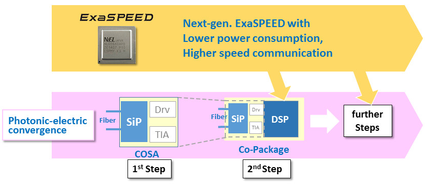
Fig. Roadmap for Key Device Development